Current characteristics of nanocrystalline silicon powder, produced by high-temperature plasma chemical synthesis
UDC
53.096, 53.097Abstract
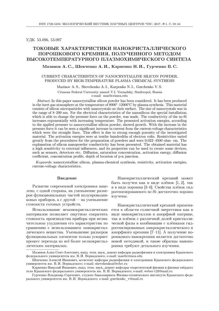
In this paper nanocrystalline silicon powder has been considered. It has been produced in the inert gas atmosphere at the temperature of 8000°-12000 °C by plasma synthesis. This material consists of silicon microparticles with nanocrystals on their surface. The size of nanocrystals was in the range of 8-200 nm. For the electrical characteristics of the nanosilicon the special installation, which is able to change the pressure force on the powder, was made. The conductivity of the nc-Si increases exponentially with increasing temperature. The presented activation energies, according to the applied pressure to nanocrystalline silicon powder, showed growth. With the increase in the pressure force it can be seen a significant increase in current from the current-voltage characteristics which were the straight lines. This effect is due to strong enough porosity of the investigated material. The activation energies were at tenths-hundredths of electron volts. Resistivities varied greatly from the procedures for the preparation of powders and were 0.022-4500 ohm$\cdot$ cm. The explanation of silicon nanopowder conductivity has been presented. The obtained material has a high sensitivity to external influences, and its properties can be used to create some devices, such as sensors, detectors etc. Diffusion, saturation concentration, activation energy, diffusion coefficient, concentration profile, depth of location of p-n junction.
Keywords:
nanocrystalline silicon, plasma-chemical synthesis, resistivity, activation energies, current-voltage characteristicsReferences
- Sennikov P.G., Golubev S.V., Shashkin V.I. [et. al.]. Fabrication of nanocrystalline silicon layers by plasma enhanced chemical vapor deposition from silicon tetrafluoride. Semiconductors, 2009, vol. 43, iss. 7, pp. 968-972.
- Pevtsov A.B., Feoktistov N.A. Plyonki nanokristallicheskogo kremniya, poluchennyye metodom mikrovolnovogo plazmohimicheskogo gazofaznogo osazhdeniya v usloviyah impulsnoy modulyatsii moschnosti razryada [Nanocrystalline silicon films prepared by microwave plasma chemical vapor deposition in the discharge power width modulation]. Pisma v ZhTF [Letters to the JTPh], 2002, vol. 28, iss. 7, pp. 89-94.
- Yefremov M.D., Arzhannikova S.A., Volodin V.A. [et al.]. Nanometrovyye klastery i nanokristally kremniya [Nanometer clusters and silicon nanocrystals]. Vestnik NGU.Seriya: Fizika [Vestnik of NGU. Series: Physics]. 2007, vol. 2, iss. 2, pp. 51-60.
- Karlach A.Yu., Kuznetsov G.V., Litvinenko S.V. [et al.]. The effect of the dynamic adsorption mode on impedance of composite structures with porous silicon. Semiconductors, 2010, vol. 44, iss. 10, pp. 1387-1393.
- Kononov N.N., Kuz'min G.P., Orlov A.N. [et al.]. Optical and electrical properties of thin wafers fabricated from nanocrystalline silicon powder. Semiconductors, 2005, vol. 39, iss. 7, pp. 868-873.
- Gribov B.G., Zinovyev K.V., Kalashnik O.N. [et al.] Sposob polucheniya kremniya vysokoy chistoty [A method for producing high purity silicon]. Pat. 2497753 Rossiyskaya Federatsiya, 2013.
- Wronski C.R., Collins R.W. Phase engineering of a-Si:H solar cells for optimized performance. Solar Energy, 2004, vol. 77, pp. 877-885.
- Juneja S., Sudhakar S., Khonina S.N. [et al.]. Nanocrystalline Silicon Thin Films and Grating Structures for Solar Cells. Proceedings of SPIE, 2016, vol. 9807, 98070F.
- Lee J.E., Ahn S.K., Park J.H. [et al.]. Boron-doped hydrogenated silicon carbide alloys containing silicon nanocrystallites for highly efficient nanocrystalline silicon thin-film solar cells. Progress in Photovoltaics: Research and Applications, 2015, vol. 23, iss. 12, pp. 1715-1723.
- Seif J.P., Descoeudres A., Nogay G. [et al.]. Strategies for Doped Nanocrystalline Silicon Integration in Silicon Heterojunction Solar Cells. IEEE Journal of Photovoltaics, 2016, vol. 6, iss. 5, pp. 1132-1140.
- Touati H., Amiri B., Sebbak A.C. [et. al.]. A numerical simulation of the effect of buffer layer band gap on the performances of nc-Si : H based solar cells. Journal of Nano- and Electronic Physics, 2016, vol. 8, iss. 2, 02008.
- Mazinov A.S., Shevchenko A.I., Voskresenskiy V.M. [et al.]. Nanostrukturirovannyye poluprovodniki, poluchennyye poroshkovym metodom [Nanostructured semiconductors obtained by the powder method]. Uchonyye zapiski Tavricheskogo natsionalnogo universiteta imeni V.I. Vernadskogo. Seriya "Fiziko-matematicheskiye nauki" [Scientific notes of Taurida National V.I. Vernadsky University. Series "Physics and Mathematics Sciences"]. 2014, vol. 27 (66), no. 2, pp. 107-114.
- Mazinov A.S., Shevchenko A.I., Voskresenskiy V.M. [et al.]. Kremniyuglerodnyye struktury dlya sovremennoy mikro- i nanoelektroniki [Silicon-carbon structures for modern micro- and nanoelectronics]. Materialy 25-y Mezhdunarodnoy Krymskoy Konferentsii "SVCh-tekhnika i telekommunikatsionnyye tekhnologii (KryMiKo'2015)" [25th International Crimean Conference Microwave {\&} Telecommunication Technology (CriMiCo'2015). Conference Proceedings]. Sevastopol, Veber Publ., 2015, pp. 689-690.
- Mazinov A.S., Shevchenko A.I., Voskresenskiy V.M., Kuropatrin A.I. Nanostrukturnyye poluprovodniki na osnove poroshkovoy tehnologii [Nanostructural semiconductors based on powder technology]. Materialy 24-y Mezhdunarodnoy Krymskoy Konferentsii "SVCh-tekhnika i telekommunikatsionnyye tekhnologii (KryMiKo'2014)" [24th International Crimean Conference Microwave {\&} Telecommunication Technology (CriMiCo'2014). Conference Proceedings]. Sevastopol, Veber Publ., 2014, pp. 740-741.
- Bahov V.A., Mazinov A,S., Nazdyorkin Ye.A., Pisarenko L.D. Vliyaniye strukturnoy neodnorodnosti na provodimost poluprovodnikovyh materialov [The impact of structural heterogeneity on the conductivity of semiconductor materials]. Elektronika i svyaz [Electronics {\&} Communications]. 2011, vol.4 (63), pp. 11-14.
Downloads
Issue
Pages
Submitted
Published
How to Cite
Copyright (c) 2017 Mazinov A.S., Shevchenko A.I., Karpenko N.I., Gurchenko V.S.

This work is licensed under a Creative Commons Attribution 4.0 International License.


